
Introduction
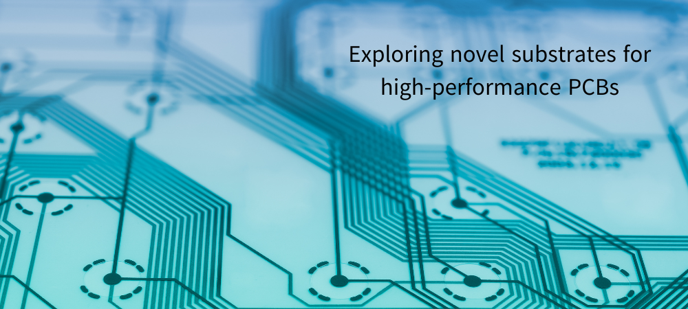
The circuits that connect components in today’s electronic products are more advanced than ever – and so are the materials that make them. Driven by the relentless pace of miniaturisation, today’s PCBs incorporate new and innovative materials to improve performance in the face of increasing numbers of components, higher speeds, smaller sizes, and every other constant challenge associated with bringing the latest electronics to market. In this article, we’ll explore the cutting-edge of one aspect of PCB reliability: advanced materials – particularly flexible and high-performance substrates. Whether you’re a technologist, PCB designer or just very curious about the technology of printed circuits, this article will reveal a lot about the technology that enables ever-smaller, more powerful, and more capable consumer electronics products.
The Evolution of PCB Materials
Traditional Substrates: A Brief Overview
Before we talk about advanced materials, let’s review the ‘traditional’ materials for making PCB:
- FR-4 (Fiberglass-reinforced epoxy laminate)
- CEM-1 and CEM-3 (Composite Epoxy Materials)
- Aluminum-based PCBs
These materials have served the industry well for decades but are limited in their ability to bend, withstand heat and perform at high frequencies.
Flexible Substrates: Bending the Rules of PCB Design
The Rise of Flexible PCBs
Flexible PCBs have revolutionized electronic product design, allowing for:
- Compact and lightweight devices
- Improved reliability in dynamic environments
- Creative form factors and 3D electronic assemblies
Key Materials for Flexible PCBs
- Polyimide (PI): The king of flexible PCBs, with high stability of thermal and mechanical properties.
- Polyethylene Terephthalate (PET): Low cost and good flex and electrical properties for less demanding applications.
- Liquid Crystal Polymer (LCP) – Good high frequency applications (low ε’ and tan δ).
- Polyethylene Naphthalate (PEN): Balancing performance and cost, suitable for mid-range flexible PCB applications.
Advantages of Flexible Substrates
- Resistance to vibration and mechanical stress
- Improved heat dissipation
- Space and weight savings in compact devices
- Enhanced design freedom for product engineers
High-Performance Substrates: Pushing the Boundaries of PCB Capabilities
As more and more electronic devices run at higher and higher microwave frequencies, and produce more and more heat, conventional substrates can no longer do what they are supposed to do. New families of high-performance substrates will pave the way for next-generation electronic products.
Key High-Performance Substrate Materials
- Rogers Materials:
- RO4000 series: Ideal for high-frequency applications up to 10 GHz
- RT/duroid series: Suitable for microwave and millimeter-wave frequencies
- PTFE (Polytetrafluoroethylene) Composites:
- Excellent dielectric properties
- Low loss at high frequencies
- Stable across a wide temperature range
- Ceramic-Filled Hydrocarbon Materials:
- Taconic TLY and TLX series
- Isola Astra MT77
- Combine high-frequency performance with ease of fabrication
- Low-Loss Glass Reinforced Hydrocarbon/Ceramic Laminates:
- Panasonic Megtron 6
- Isola I-Tera MT40
- Ideal for high-speed digital and high-frequency RF applications
Advantages of High-Performance Substrates
- Superior electrical performance at high frequencies
- Improved thermal management
- Enhanced signal integrity
- Reduced signal loss and crosstalk
Emerging Trends in PCB Substrate Materials
Biodegradable and Eco-Friendly Substrates
Alongside environmental concerns, scientists are working to make PCB materials more sustainable, and even biodegradable, including:
- Paper-based substrates
- Bioplastic composites
- Recycled and renewable material blends
These greener solutions for hardware offloading can boost tool sustainability by decreasing the human impacts of electronic waste – while lesser-minded applications.
Nanomaterial-Enhanced Substrates
Incorporating nanomaterials into PCB substrates can dramatically improve their properties:
- Carbon nanotubes for enhanced thermal conductivity
- Graphene for improved electrical performance
- Nanoparticle-infused resins for tailored dielectric properties
Thus, through the nanocomposites, a substrate can be tailor-fit at the molecular level to suit PCB performance.
Smart and Responsive Materials
The future of PCB substrates may include materials that can adapt to their environment:
- Self-healing polymers to repair minor damage
- Thermochromic materials for visual temperature indication
- Piezoelectric substrates for energy harvesting in IoT devices
Hybrid and Multi-Material Substrates
One of the most exciting areas of PCB materials innovation is the development of ‘hybrid substrates’ that benefit from the best features of multiple materials:
- Rigid-flex boards with both flexible and rigid sections
- Ceramic-polymer composites for improved thermal management and electrical performance
- Multi-layer structures with tailored properties for each layer
Such hybrid solutions let designers fine-tune PCB performance to optimise certain parts of the board while reducing cost by limiting expensive technology to the critical areas.
Challenges and Considerations in Advanced PCB Materials
While advanced materials offer exciting possibilities, they also present challenges:
- Cost: High-performance and flexible substrates are often more expensive than traditional options.
- Manufacturability: Some advanced materials require specialized equipment and processes.
- Depends on Design Complexity: Designing very high-frequency circuits or flexible circuits requires an awareness of materials properties.
- Reliability Testing: New materials require extensive testing to ensure long-term performance and reliability.
- Poor Continuity: There can be issues with supply chain continuity when dealing with specialty materials. This holds especially true for low-volume production runs.
- Regulatory compliance: Using new materials can make testing for environmental and safety compliance more difficult.
- Compatibility with Older Technology: It could be necessary to install new substrate materials, which would necessitate the adaptation of soldermask or other manufacture stages or component attachment methods.
The Role of Simulation and Modeling in Advanced PCB Materials
In a PCB where materials and structures have a greater complexity and specialisation than ever, such a process becomes increasingly important to follow, but it becomes extremely difficult to do so. Especially since the accuracy of the simulation and modelling tools available is continually increasing. It is now possible for designers to use electromagnetic and thermal simulation software that:
- Predicts the performance of new material combinations
- Optimizes layouts for high-frequency applications
- Identifies potential issues before physical prototyping
Without such tools, the development time and cost associated with advanced PCB materials will be prohibitive in many products where performance margins are small and reliability is of paramount concern.
Conclusion: The Future of PCB Materials
The future of PCB manufacturing is already changing; a revolution is happening. The rapid advances of new technologies in communications such as 5G, Internet of Things (IoT), wearable devices, mobile phones, the need for reduced weight, smaller size and higher-performance electronics, it is all driving the revolution, though some may think that it is premature to call it that. Flexible and high-performance substrates are at the heart of the revolution and are enabling electronic equipment designers to build products that were once never thought possible.
Looking forward, PCB materials evolution will continue, perhaps driven by the following factors:
- Even higher frequency performance
- Improved thermal management
- Greater flexibility and durability
- Enhanced sustainability and eco-friendliness
Knowledge of these new PCB materials can inspire engineers and product designers to think beyond existing limitations and to push the boundaries of what’s possible in electronic device design. The smartphones of tomorrow, along with the next generation of medical devices, aerospace systems, and many other products, will be powered by truly advanced new substrate materials.
Whether you’re looking at what the next big product will be or you’re just curious about the world around you, today’s advanced PCB materials are a window into the coming electronics revolution for more information visit PCBTrace.com